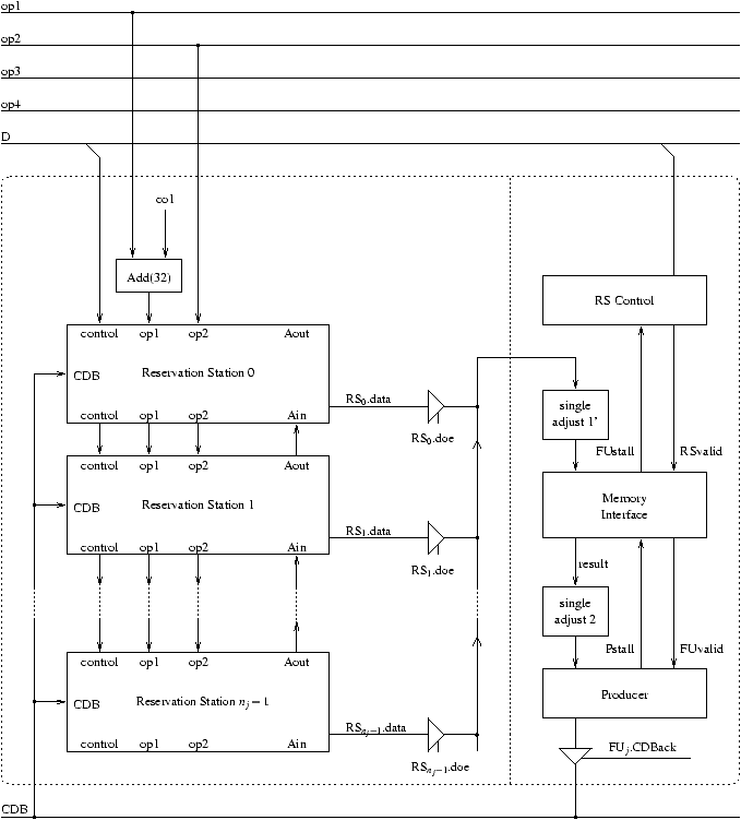
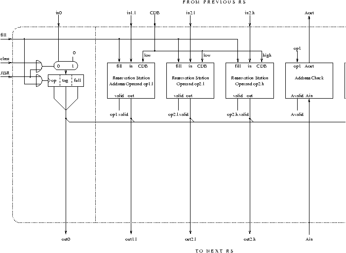
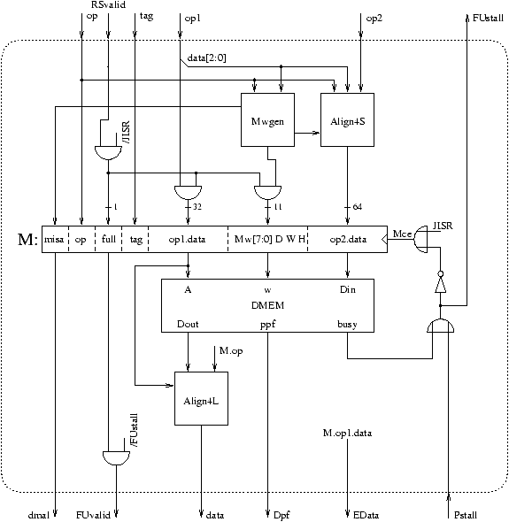
The address operand of a memory instruction is always a GPR register and it is transported in the low part of operand bus one. The immediate constant (provided by the decode/issue environment), which is used as address offset, is added to the value on this bus before it is stored in reservation station R0. If the operand is already valid during issue, the sum is the correct memory address. If not so, the decode/issue environment puts zero on the operand bus. In this case, the sum is the immediate constant.
The second operand is only used for store instructions. It holds the value to be stored. Since this can be a double precision floating point value, two reservation station operands are required, one for the low and one for the high part. The operand circuit used for operand two is identical to the operand circuit presented in chapter 3 (figure 3.15).
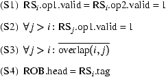
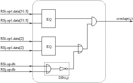
The first step in order to calculate this signal is to define the overlap(i,j) macro (figure 4.6). In the given implementation, only two different memory operand widths are considered, which are 64-bit and 32-bit. Halfword and byte wide operands are handled as 32-bit operands. In order to determine this operand with, the macro DB(i,j) is used. It is true iff at least one of the operands in RSi or RSj is a double precision value. The test for overlapping operands is done as follows: In case of single precision values, address bits 2 to 31 are compared. If double precision values are involved, address bits 3 to 31 are compared.
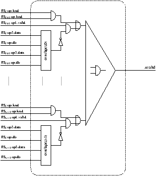
Figure 4.5: The data memory reservation station address comparator operand for reservation station RSi
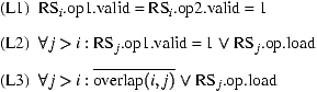
| overlap(i,j) | = | (RSi.op1.data[31:3] = RSj.op1.data[31:3]) Ù |
| ((RSi.op1.data[2] = RSj.op1.data[2]) Ú /DB(i,j)) |
RSi:

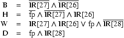
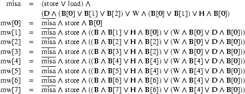
The memory is accessed by a 64-bit wide data path. In order to store single bytes, halfwords and words, the memory interface uses eight bank write signals mw[7:0]. These bank write signals are calculated by the Mwgen circuit, which is taken from [Lei98]. The first step is to determine the exact width of the operand. For this purpose, the bits B (byte), H (halfword), W (word), and D (doubleword) are calculated from bits of the instruction word.


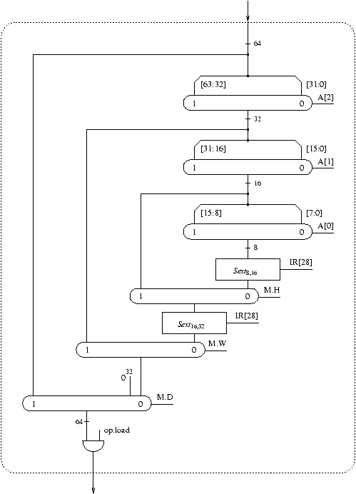
The align-for-load (Align4L) circuit (figure 4.9) performs the alignment shift after a load instruction. The first step is to select the bits of the memory operand from the 64-bit memory bus. This is done by three cascaded multiplexers, which are controlled by the address bits A[2:0]. The first multiplexer selects the correct 32-bit word from the 64-bit bus. The second multiplexer selects the correct 16-bit halfword from the 32-bit word generated by the first multiplexer. The third multiplexer selects the correct byte from this halfword.
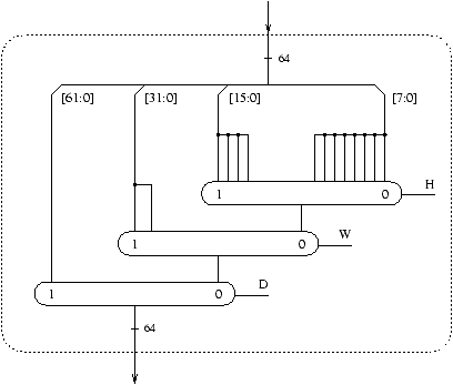
The align for store (Align4S) circuit (figure 4.10) is much simpler. The operand provided by the single-adjust-one circuit is copied on all valid locations on the 64-bit memory bus. Three multiplexers select the operand with the correct width.