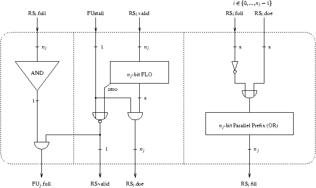
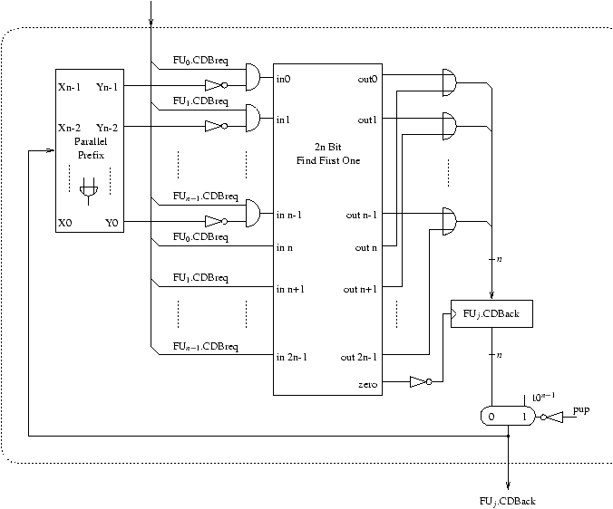
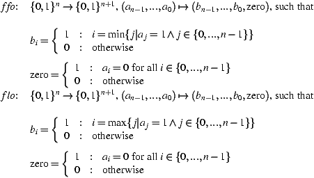
Furthermore, the hardwired control described in this chapter requires two additional basic circuits: the n-bit find first one circuit (FFO) and the find last one circuit (FLO). They calculate the following functions:
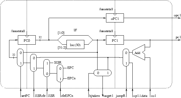
Usually, the new value of the PC0 register is the old value incremented by four. In case of a branch, rfe, jump or an interrupt, the PC register has to be clocked with another value. In these cases, the setPC signal is set. The signal is calculated as follows:
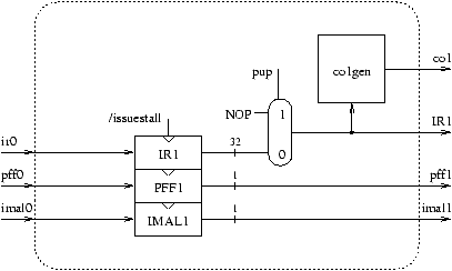
During an issue stall (issuestall=1), all clock enable signals are disabled in order to prevent modifications of the PC registers.
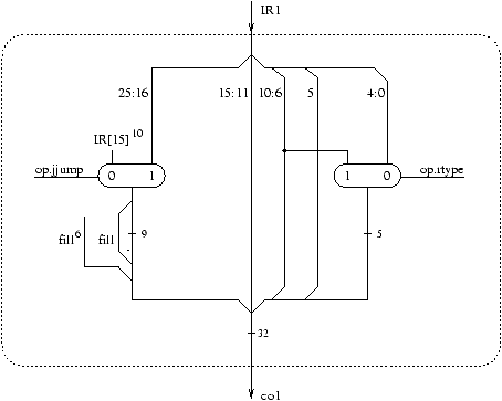
For some instructions, the instruction word provides an immediate constant. The instruction register environment contains the co1gen circuit (figure 3.7), which extracts the immediate constant from the instruction in IR1 and performs a sign extension to 32 bits (signal co1). It is literally taken from [MP95]. The op.jjump and op.rtype signals are generated by the decode/issue environment and are used to determine the width of the constant and the position in the instruction word.
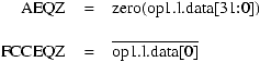
Target Active control Monomials state signals IR[31:26] IR[6] IR[5:0] ALU rtype, FU.alu 000000 * 0001** 000000 * 10**** Shifti rtype, FU.alu 000000 * 0000** ALUi itype, FU.alu 0*1*** * ****** Load itype, load, FU.mem 100*** * ****** Load.s itype, load, fp, FU.mem 110001 * ****** Load.d itype, load, fp, db, FU.mem 110101 * ****** Store itype, store, FU.mem 101*** * ****** Store.s itype, store, fp, FU.mem 111001 * ****** Store.d itype, store, fp, db, FU.mem 111101 * ****** Faddsub.s rtype, faddsub, fp, FU.fadd 010001 0 00000* Faddsub.d rtype, faddsub, fp, db, FU.fadd 010001 1 00000* Fmul.s rtype, fmul, fp, FU.fmul 010001 0 000010 Fmul.d rtype, fmul, fp, db, FU.fmul 010001 1 000010 Fdiv.s rtype, fdiv, fp, FU.fdiv 010001 0 000011 Fdiv.d rtype, fdiv, fp, db, FU.fdiv 010001 1 000011 Fcond.s rtype, fcc, fp, FU.ftest 010001 0 11**** ID1 Fcond.d rtype, fcc, fp, FU.ftest 010001 1 11**** Fabsneg.s rtype, fabsneg, fp, FU.fconv 010001 0 00010* Fabsneg.d rtype, fabsneg, fp, db, FU.fconv 010001 1 00010* Ff2i rtype, ff2i, fp, FU.fconv 010001 * 001001 Fi2f rtype, fi2f, fp, FU.fconv 010001 * 001010 FMov.s rtype, fmov, fp, FU.fconv 010001 0 001000 FMov.d rtype, fmov, fp, db, FU.fconv 010001 1 001000 FConv.s rtype, fconv, fp, FU.fconv 010001 * 100*00 FConv.d rtype, fconv, fp, db, FU.fconv 010001 * 100001 Branch itype, bjjr, branch, noFU 00010* * ****** FBranch itype, bjjr, branch, fp, noFU 00011* * ****** JumpReg itype, bjjr, bjtaken, jumpR, noFU 010110 * ****** Jump&LinkReg itype, jalr, bjtaken, jumpR, noFU 010111 * ****** Jump jtype, bjjr, bjtaken, jump, noFU 000010 * ****** Jump&Link jtype, jalr, bjtaken, jump, noFU 000011 * ****** Trap jtype, trap, noFU 111110 * 000000 RFE jtype, rfe, noFU 111111 * ****** Movs2i rtype, movs2i, FU.alu 000000 * 010000 Movi2s rtype, movi2s, FU.alu 000000 * 010001 FUnimp iuFOP, noFU 010001 * 00011* 010001 * 01**** Illegal (z0) ill, noFU - Taken bjtaken AEQZ · /IR1[26] /AEQZ · IR1[26] ID2 FCCEQZ · /IR1[26] /FCCEQZ · IR1[26] Untaken /taken
State Instructions op1. op2. op3. op4. dest. ALU add, sub, test/set, shift RS1 RS2 - - RD ALUi addi, subi, test/set immediate RS1 imm - - RD Shifti shift with shift amount RS1 imm - - RD Load load GPR RS1 - - - RD Load.s load single precision FPR RS1 - - - FD Load.d load double precision FPR RS1 - - - FD Store store GPR RS1 RD - - - Store.s store single precision FPR RS1 FD - - - Store.d store double precision FPR RS1 FD - - - Faddsub.s fadd.s, fsub.s FS1 FS2 RM MASK FD Faddsub.d fadd.s, fsub.s FS1 FS2 RM MASK FD Fmul.s fmul.s FS1 FS2 RM MASK FD Fmul.d fmul.d FS1 FS2 RM MASK FD Fdiv.s fdiv.s FS1 FS2 RM MASK FD Fdiv.d fdiv.d FS1 FS2 RM MASK FD Fcond.s fc.cond.s FS1 FS2 - MASK FCC Fcond.d fc.cond.d FS1 FS2 - MASK FCC Fabsneg.s fabs.s, fneg.s FS1 - - - FD Fabsneg.d fabs.d, fneg.d FS1 - - - FD Ff2i mf2i FS1 - - - RS2 Fi2f mi2f RS2 - - - FS1 FMov.s mov.s FS1 - - - FD FMov.d mov.d FS1 - - - FD FConv.s cvt.s.d, cvt.s.i, cvt.i.s, cvt.i.d FS1 - - - FD FConv.d cvt.d.i, cvt.d.s FS1 - - - FD Branch beqz, bnez RS1 - - - - FBranch fbeqz, fbnez FCC - - - - JumpReg jr RS1 - - - - Jump&LinkReg jalr RS1 - - - R31 Jump j - - - - - Jump&Link jal - - - - R31 Trap trap - - - - - RFE rfe - - - - - Movs2i movs2i SA - - - RD Movi2s movi2s RS1 - - - SA

FU Purpose FU[0] = FU.alu integer instructions, movi2s, movs2i FU[1] = FU.mem load, store FU[2] = FU.fadd floating point addition and substraction FU[3] = FU.fmul floating point multiplication FU[4] = FU.fdiv floating point division FU[5] = FU.fconv conversion floating point / integer FU[6] = FU.ftest floating point condition tests
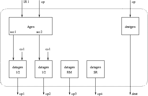
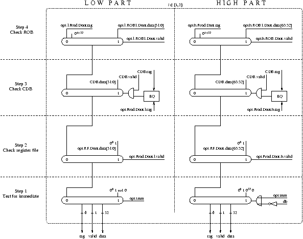
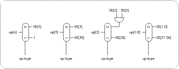
The operand address generation circuit Agen (figure 3.10) calculates the types and addresses of the source registers. For each operand, the operation generation environment opgen provides signals, which point to bit fields in the instruction word. In turn, these bit fields contain the register addresses of the operands. The type of an operand is represented by five signals:
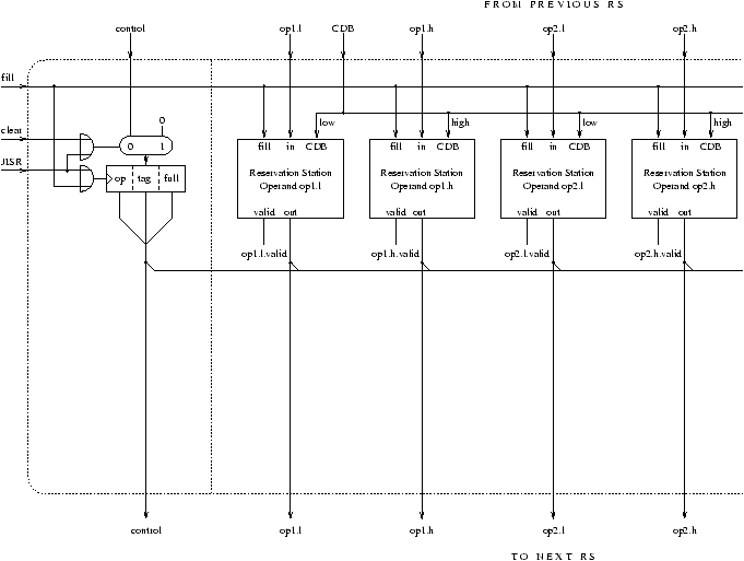
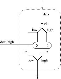
Bus Items Width Purpose op1 l J+32+1 low part of the first operand h J+32+1 high part of the first operand high 1 lowest bit of the register address op2 l J+32+1 low part of the first operand h J+32+1 high part of the first operand high 1 lowest bit of the register address op3 l J+32+1 third operand (always integer) op4 l J+32+1 fourth operand (always integer)
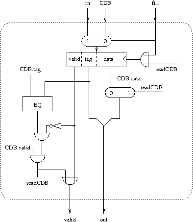
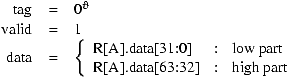
Item Width Purpose tag J ROB tag of the instruction producing the operand valid 1 valid =1 Û operand contains valid data data 32 actual operand data


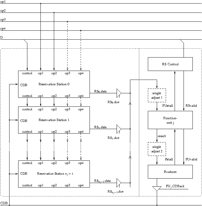
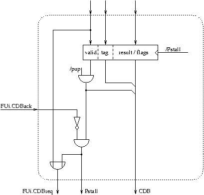
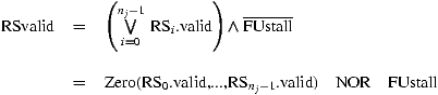
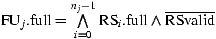
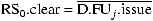
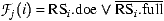
The reservation stations form a queue for instructions and their operands which are provided on the op1 to op4 busses. These busses originate in the decode/issue environment. In each cycle, any desired instruction can move from its reservation station into the function unit. For this purpose, all reservation stations are connected to a bus with tristate drivers. The bus and the reservation stations are controlled by the reservation station control.

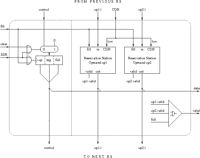
Furthermore, the valid signal of the reservation station operand becomes active in the same cycle in which readCDB is active. This allows dispatching instructions in the same cycle they received their operands via the CDB. This is a performance optimization only and does not affect correctness.
RSi.opx RSi-1.opx new value of fill readCDB readCDB RSi.opx.data 0 0 * RSi.opx.data 0 1 * CDB.data 1 * 0 RSi-1.opx.data 1 * 1 CDB.data

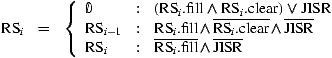
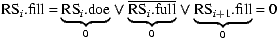
RSnj-2.full RSnj-1.full RSnj-2.doe RSnj-1.doe RSnj-1.clear RSnj-1.fill action in RSnj-1 0 0 0 0 0 1 copy previous RS, which is empty 0 1 1 0 not possible 1 1 0 1 0 0 0 0 no action 0 1 0 1 copy previous RS, which is empty 1 0 not possible 1 1 not possible 1 0 0 0 0 1 copy instruction in previous RS 0 1 not possible 1 0 1 1 clear RS, although already empty 1 1 not possible 1 1 0 0 0 0 no action 0 1 0 1 replace the current instruction with instruction in previous RS 1 0 1 0 no action 1 1 not possible


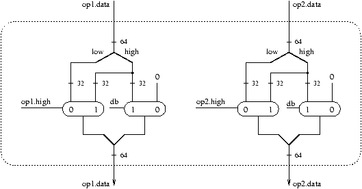
Inputs Result high db low part high part 0 0 data[31:0] 032 1 0 data[63:32] 032 0 1 data[31:0] data[63:32] 1 1 not possible
Table 3.8: Single adjust before function unit for one operand. The input from the reservation is data[63:0].
After leaving the function unit, the single-adjust-two circuit between the function unit and the producer part of the reservation station reverts this procedure. It ensures that a single precision result is both on the low and on the high part of the CDB to avoid any possible alignment problems. The implementation is given in figure 3.19.

Bus Items Width Purpose CDB tag J ROB tag of the instruction producing the result valid 1 CDB.valid=1 Û CDB contains valid data data 64 actual result mal 1 misaligned memory access Dpf 1 page fault during data memory access ovf 1 overflow in ALU instruction IEEEf 5 IEEE conforming floating point flags EData 32 exception data
op[4] op[3] op[2] op[1] op[0] Function 0 0 0 0 0 a << b 0 0 0 1 0 a >> b 0 0 0 1 1 a >> b (arithmetic) 1 0 0 0 0 a+b with test of overflow 1 0 0 0 1 a+b without test of overflow 1 0 0 1 0 a-b with test of overflow 1 0 0 1 1 a-b without test of overflow 1 0 1 0 0 a Ù b 1 0 1 0 1 a Ú b 1 0 1 1 0 a Å b 1 0 1 1 1 b[0:15] 016 1 1 0 0 1 a > b ? 1 : 0 1 1 0 1 0 a = b ? 1 : 0 1 1 0 1 1 a ³ b ? 1 : 0 1 1 1 0 0 a < b ? 1 : 0 1 1 1 0 1 a ¹ b ? 1 : 0 1 1 1 1 0 a £ b ? 1 : 0
The implementation of floating point units is beyond this thesis. The actual operation performed by the FU is determined by IR[8:0]. These bits are forwarded to the reservation station during issue as part of the op bits.
Purpose Latency # RS floating point addition and substraction 5 2 floating point multiplication 5 2 floating point division 15 1 conversion floating point / integer 4 1 floating point condition tests 1 1
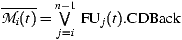
| R(t) | = | { i Î {0,...,n-1} | FUi(t).CDBreq = 1 } |
| A(t) | = | { i Î {0,...,n-1} | FUi(t).CDBack = 1 } |
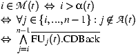
| j Î ( R(t) Ç M(t)) | Û | (j Î R(t)) Ù (j Î M(t)) |
| ( R(t) Ç M(t))j | = | Rj(t) Ù Mj(t) |


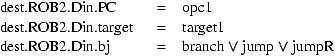
Name Width ROB Purpose valid 1 ROB1 valid =1 Û data contains a valid value data 64 ROB1 result data dmal 1 ROB1 misaligned data memory access Dpf 1 ROB1 data memory page fault ovf 1 ROB1 overflow in ALU instruction IEEEf 5 ROB1 IEEE flags (only used by floating point instr.) EData 32 ROB1 exception data å 105 ill 1 ROB2 illegal instruction imal 1 ROB2 misaligned instruction memory access Ipf 1 ROB2 instruction memory page fault trap 1 ROB2 trap =1 Û instruction is a trap instruction uFOP 1 ROB2 unimplemented floating point instruction dest 4 ROB2 destination register address db 1 ROB2 db =1 Û result has double precision fpr 1 ROB2 fpr =1 Û dest is a floating point register spr 1 ROB2 spr =1 Û dest is a special purpose register gpr 1 ROB2 gpr =1 Û dest is a general purpose register PC 32 ROB2 PC of the instruction target 32 ROB2 target / fallthrough address bj 1 ROB2 bj =1 Û instruction is a branch/jump å 78
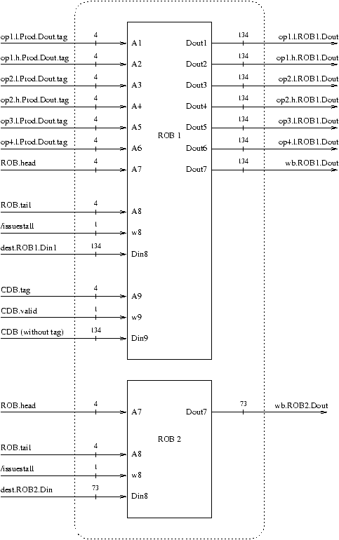
Port Use Purpose 1 read only ROB1 Forwarding of low part of operand 1 2 read only ROB1 Forwarding of high part of operand 1 3 read only ROB1 Forwarding of low part of operand 2 4 read only ROB1 Forwarding of high part of operand 2 5 read only ROB1 Forwarding of operand 3 6 read only ROB1 Forwarding of operand 4 7 read only ROB1, ROB2 Retire 8 write only ROB1, ROB2 Issue (destination) 9 write only ROB1 Completion
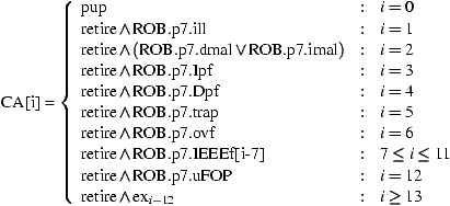
Interrupt Symbol Priority Resume Maskable External reset reset 0 abort no yes illegal instruction ill 1 abort no misaligned access mal 2 page fault IM Ipf 3 repeat page fault DM Dpf 4 trap trap 5 continue FXU overflow ovf 6 continue yes no FPU overflow fOVF 7 FPU underflow fUNF 8 abort/ FPU inexact result fINX 9 continue FPU divide by zero fDBZ 10 FPU invalid operation fINV 11 FPU unimplemented uFOP 12 continue no external I/O exj 12+j continue yes yes
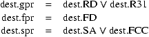
| wb.A | = | wb.ROB2.Dout.dest |
| wb.gpr | = | wb.ROB2.Dout.gpr |
| wb.fpr | = | wb.ROB2.Dout.fpr |
| wb.spr | = | wb.ROB2.Dout.spr |
| wb.db | = | wb.ROB2.Dout.db |
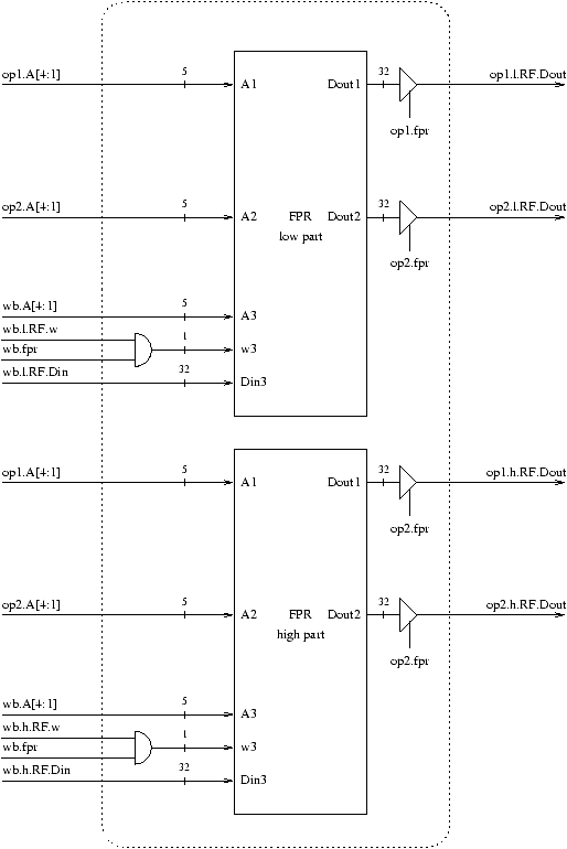
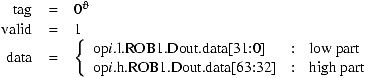
| wb.l.RF.Din | = | wb.ROB1.Dout.data[31:0] |
| wb.h.RF.Din | = | wb.ROB1.Dout.data[63:32] |
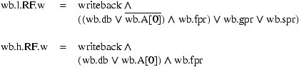
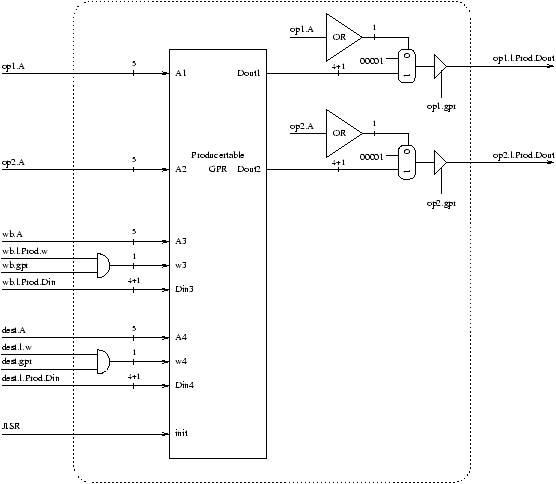
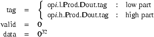
| wb.l.Prod.w | = | wb.l.RF.w Ù (wb.l.Prod.Dout.tag=ROB.head) |
| wb.h.Prod.w | = | wb.h.RF.w Ù (wb.h.Prod.Dout.tag=ROB.head) |
| wb.l.Prod.Din.valid | = | 1 |
| wb.l.Prod.Din.tag | = | 0J |
| wb.h.Prod.Din.valid | = | 1 |
| wb.h.Prod.Din.tag | = | 0J |
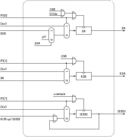
| ESR | = | SR |
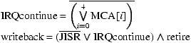
| ECA | = | MCA |
| SR | = | 0 |
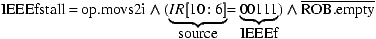
| EDATA | = | ROB[ROB.head].Edata |
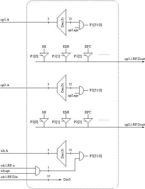
Nr. Name Purpose 0 SR Status register (interrupt mask) 1 ESR Exception status register 2 EPC Exception program counter 3 EPCn Exception program counter 2 4 ECA Exception cause register 5 EData Exception data register 6 RM Floating point rounding mode 7 IEEEf IEEE interrupt flags 8 FCC Floating point comparison flag
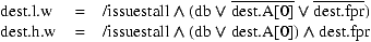
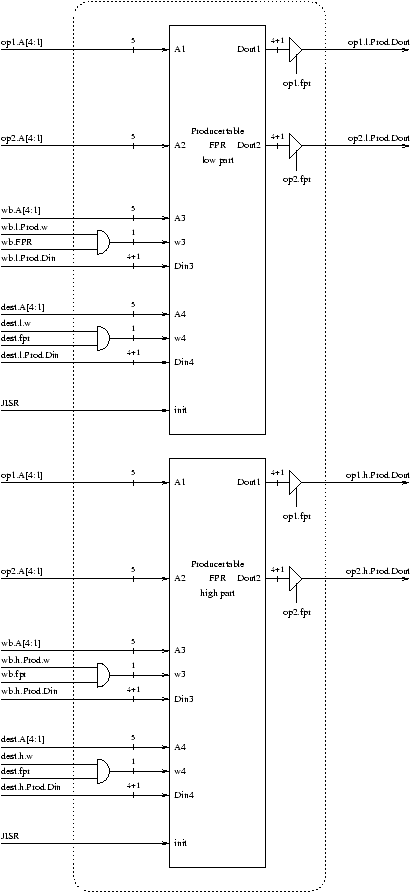
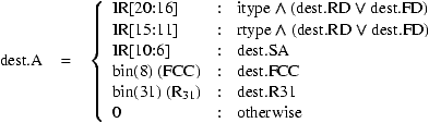
| Dest.l.Prod.Din.valid | = | 0 |
| Dest.l.Prod.Din.tag | = | ROB.tail |
| Dest.h.Prod.Din.valid | = | 0 |
| Dest.h.Prod.Din.tag | = | ROB.tail |